
Key Highlights
-
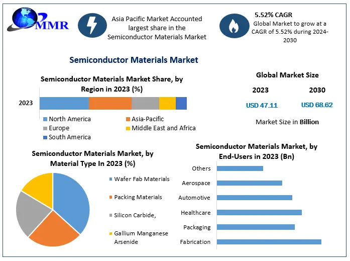
Advanced fab materials command the primary share of the global electronics chemical supply architecture.
-
Lithography and advanced photoresists represent the fastest-growing process chemical sub-segment.
-
The Asia-Pacific region maintains absolute volume dominance across primary wafer fabrication materials.
-
Sub-2nm manufacturing processes require ultra-high-purity (UHP) chemical formulations exceeding 9N purity.
-
Advanced packaging materials are expanding rapidly due to chiplet design architectures.
Why This Matters Now
The structural architecture of global chemical procurement is undergoing an irreversible disruption as advanced node semiconductor manufacturing outpaces legacy chemical supply chains. Industrial buyers and chemical procurement leaders can no longer rely on cross-border spot-market sourcing to secure specialized precursor materials. The rapid deployment of next-generation artificial intelligence accelerators and high-performance computing clusters requires an immediate, capital-intensive redesign of the chemical manufacturing footprint.
Every advanced fabrication facility under construction globally creates an immediate downstream supply vulnerability for specialized chemical suppliers who fail to align their raw material capacities with local fab timelines. This supply-demand friction forces chemical manufacturing executives to choose between multi-million dollar regional capacity expansions or risking market share exclusion.
Market Overview
The Semiconductor Materials Market comprises the highly specialized chemical formulations, gas mixtures, substrates, and polishing slurries required to manufacture integrated circuits. This sector is split into front-end fabrication materials and back-end packaging materials. Front-end materials include silicon wafers, photoresists, wet process chemicals, gases, and chemical mechanical planarization (CMP) slurries. Back-end materials cover leadframes, organic substrates, ceramic packages, bonding wires, and encapsulation resins.
The industry operates under extreme technical performance tolerances where minor chemical impurities cause systemic wafer defects. To minimize these risks, manufacturers are building dedicated electronic chemical production lines near major fabrication clusters.
Key Trends Driving Growth
The primary catalyst for market re-engineering is the transition toward sub-2nm logic gates and complex 3D NAND flash memory architectures. These advanced fabrication processes require a complete redesign of traditional chemical deposition and etching steps. High-aspect-ratio etching demands specialized fluorinated gas chemistries that can penetrate deep into silicon architectures without damaging neighboring structures. This technical requirement shifts market demand from standard commodity chemicals to low-volume, high-margin specialty formulations.
Simultaneously, the widespread adoption of Extreme Ultraviolet (EUV) lithography has altered the commercial landscape for structural photoresists and developer solutions. Traditional chemical-amplified resists face physical limitations at narrower line-widths, driving the development of metal-oxide photoresists. These organometallic formulations offer superior etch selectivity and line-edge roughness control, creating a high-growth niche for specialized chemical manufacturers.
Furthermore, advanced packaging trends are changing the volume requirements for back-end materials. As physical scaling limits traditional monolithic silicon design, device manufacturers are turning to chiplet architectures and 2.5D/3D packaging. This transition drives a significant increase in demand for high-density organic substrates, epoxy mold compounds, and specialized underfill materials.
Segment Insights
-
Fabrication Materials (Dominant Segment): Front-end process inputs, led by high-purity silicon wafers and electronic specialty gases, command the largest portion of overall market capital allocation.
-
Lithography & Ancillary Chemicals (Fastest-Growing Segment): Driven by EUV deployment and advanced multi-patterning protocols, the specialized photoresist and developer division is seeing the fastest revenue acceleration.
-
Chemical Mechanical Planarization (CMP): This segment maintains stable volume expansion as multi-layer transistor stacking requires highly selective colloidal silica and ceria polishing slurries.
-
Gases & Precursors: This division is expanding rapidly due to the increased use of atomic layer deposition (ALD) and chemical vapor deposition (CVD) in advanced fabrication facilities.
Regional Growth Story
The Asia-Pacific region maintains absolute volume dominance across the semiconductor materials supply network, with Taiwan, South Korea, Japan, and China controlling key production nodes. Taiwan’s massive concentration of advanced foundry capacity creates a localized demand loop for electronic chemicals, driving international suppliers to establish regional blending facilities. Japan remains a critical supplier of core raw materials, controlling global production shares in silicon wafers, photoresists, and ultra-high-purity hydrogen fluoride.
North America is seeing significant investment activity, spurred by federal funding initiatives aimed at rebuilding domestic fabrication capacity. This regulatory shift has prompted global chemical suppliers to plan new production lines across Arizona, Ohio, and Texas to support upcoming fab nodes. Meanwhile, Europe is focused on expanding its automotive and industrial semiconductor manufacturing base, creating a steady demand pathway for specialized power semiconductor substrates like silicon carbide and gallium nitride.
Competitive Landscape
The competitive structure of the semiconductor materials market is highly consolidated, with a few specialized chemical conglomerates controlling key technological patents. Major players include Shin-Etsu Chemical Co., Ltd., Sumitomo Chemical Co., Ltd., Merck KGaA, DuPont de Nemours, Inc., Linde plc, Air Liquide, and Showa Denko K.K.
Competition centers on raw material purity levels, specialized logistics networks, and close collaborative engineering relationships with fabrication clients. Leading manufacturers are investing heavily in localized purification infrastructure to ensure their products consistently meet strict electronic specification limits.
Recent Developments
-
Chemical manufacturers have optimized their electronic gas distribution assets to accelerate high-purity precursor production for advanced logic nodes.
-
Specialty materials firms have advanced their domestic logistics infrastructure to supply ultra-pure wet chemicals directly to North American fab clusters.
-
Materials groups have expanded their exploratory cleanroom assets to develop next-generation organometallic photoresists for high-NA EUV applications.
-
Industrial gas suppliers have expanded their regional distribution agreements to secure long-term helium and neon supplies for fast-growing Asian technology hubs.
Strategic Implications
The transition toward localized, high-purity chemical manufacturing means procurement managers can no longer rely on single-source offshore production models. The high concentration of raw material manufacturing in specific geographic zones means that localized power disruptions or export controls can rapidly trigger global material shortages.
To mitigate these supply chain risks, semiconductor manufacturers are requiring material suppliers to establish multi-regional production footprints. This operational shift forces material suppliers to invest in redundant manufacturing lines, which alters historical asset utilization rates and increases baseline capital expenditure requirements.
Future Outlook
The global semiconductor materials market is positioned for sustained structural capital expansion as high-performance computing and automotive electrification drive demand for specialized chemical processing formulations. Long-term commercial success will belong to chemical suppliers that build localized purification assets near expanding fab clusters while securing reliable raw material feedstocks to protect clients from supply disruptions.
Analyst Perspective
“The semiconductor materials sector has moved beyond a standard commodity growth cycle into a phase defined by strict purity demands and localized manufacturing mandates,” states Ankita Kagawade, Lead Analyst at Maximize Market Research. “With advanced packaging and sub-2nm nodes requiring completely new chemical formulations, material suppliers must co-locate production facilities near key foundry hubs to remain competitive.”
About Maximize Market Research
Maximize Market Research Pvt. Ltd. (MMR) is a global market research and consulting company that provides reliable, data-focused, and practical business insights. The firm serves a wide range of industries, including healthcare, pharmaceuticals, technology, automotive, electronics, chemicals, personal care, and consumer goods. Through market forecasts, competitive analysis, strategic consulting, and industry impact assessments, MMR helps organizations understand changing market conditions, identify growth opportunities, and make informed business decisions for long-term success.
2nd Floor, Navale IT Park Phase 3
Pune Banglore Highway, Narhe
Pune, Maharashtra 411041, India
+91 9607365656
[email protected]